Edit ECAD data
Open an ECAD file for editing
In the PCB industry, ECAD files are commonly used to provide PCB data. You can edit PCB data on the PCB tab of the NPI Process Definition window.
Note
If CAD data exists in the file, it will open on the PCB tab; otherwise it will open on the Gerber tab of the window.If CAD data exists in the file, it will open on the PCB tab; otherwise it will open on the Gerber tab of the window.
Log into the NPI client application.
Select Process Engineering
 , then open an assembly that contains an ECAD file from the Define Processes window.
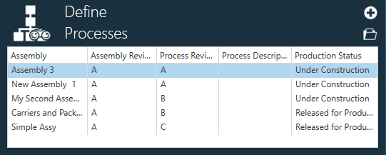
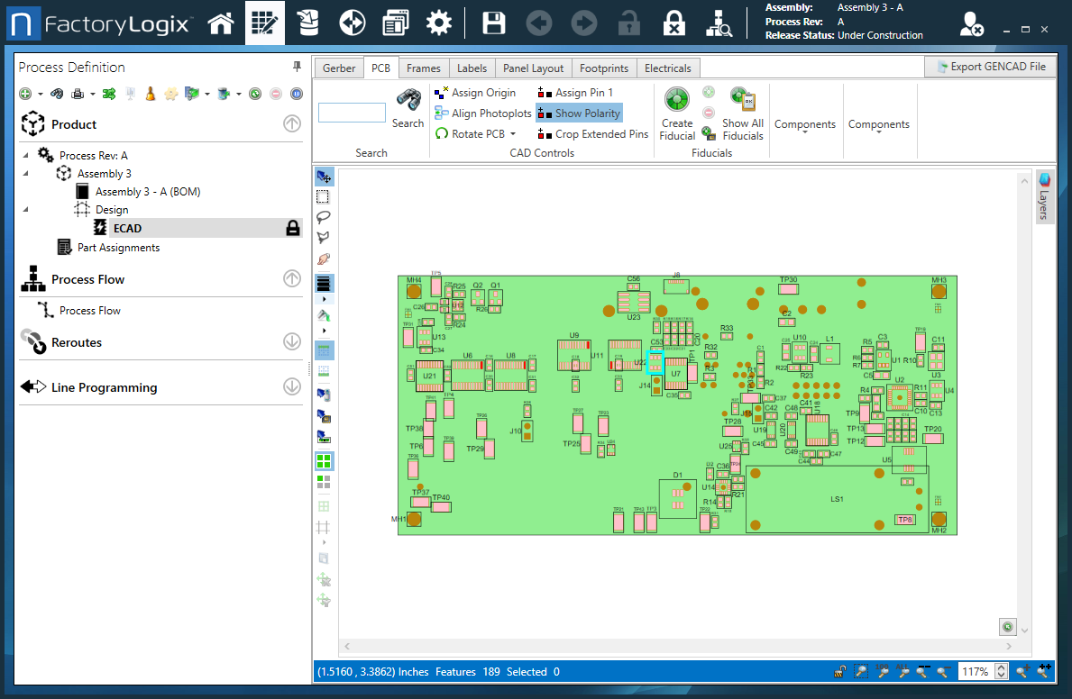
In the Process Definition window, select the ECAD file on the left side of the window to load the file.
On the left side of the Process Definition window, the Process tree displays all of the components that make up a process definition.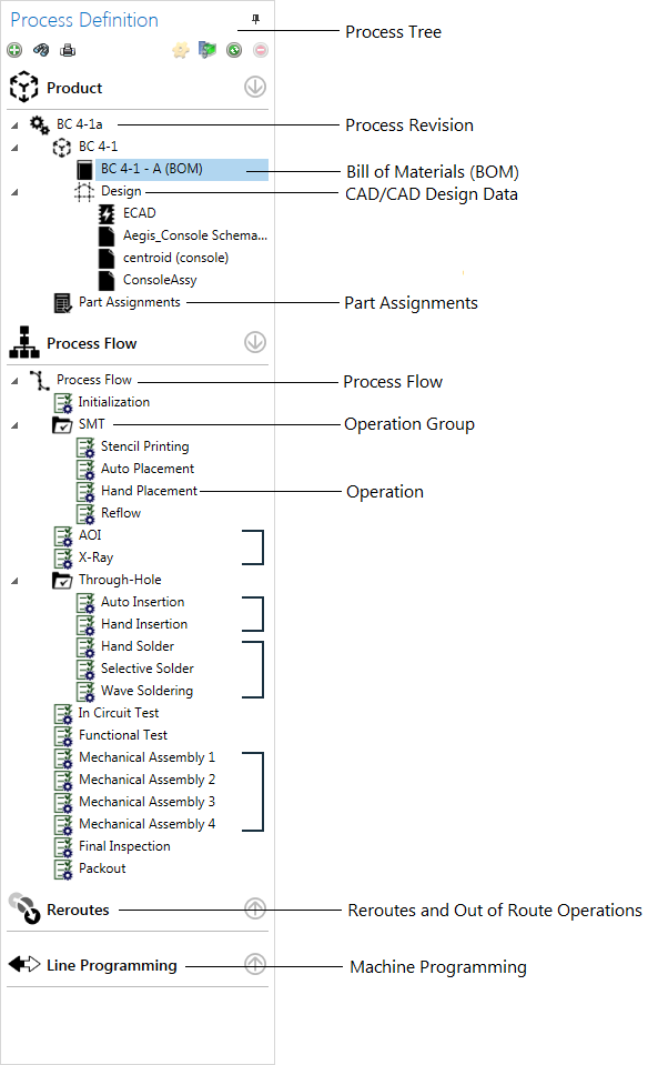
Use the tools across the top of the window to view and modify ECAD data. (The following topics describe the tabs and the tools on each tab you can use to edit ECAD data.)
Gerber tab editing tools
The Gerber tab of the Process Definition window has powerful editing tools that allow you to edit ECAD data. The tools are organized by type:
Gerber Controls
Confirmations
The following topics describe how to use the Gerber tab's tools to modify ECAD data.
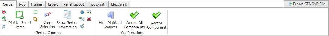
Gerber Controls tools
Tool | Description |
|---|---|
Delete Digitized Component  | Deletes the highlighted (selected) digitized object. |
Automatically Scan for Identical Components  | Scans for and identifies identical components in a Gerber file. When identified, the components are placed in a buffer so that they can also be digitized. |
Gerber Preferences  | Displays a dialog where you can specify preferences for handling Gerber files:
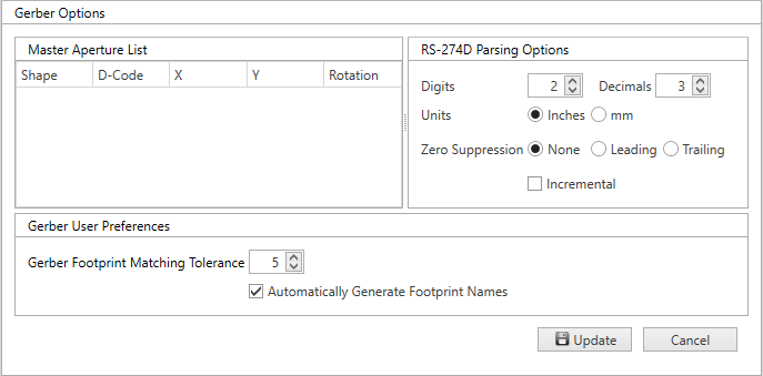 |
Digitize Board Frame  | Allows you to digitize the PCB board frame. |
Image Frame  | Used in conjunction with the Digitize Board Frame button. When the frame is digitized, it will be set as the Image (circuit) Frame. |
Panel Frame  | Used in conjunction with the Digitize Board Frame button. When the frame is digitized, it will be set as the Panel Frame. |
Clear Selection  | Clears all information in the buffer. |
Show Gerber Information  | When selected, information on the Gerber component’s pads (D-Code, Location, and so on) is displayed. |
Import Aperture List  | Displays a dialog where you can locate and select an aperture file to import. |
Show Hidden Graphics  | When selected, all objects that were previously hidden (but not deleted) are displayed. |
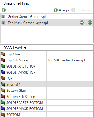
Link Gerber Files to Layers  | Allows you to link/assign Gerber files to the different layers of a PCB.
|
Delete All Hidden Data | When selected, all objects that were previously hidden are deleted permanently. |
Import Centroid File  | Displays a dialog allowing you to locate and import a Centroid file so you can assign reference designators during digitization.
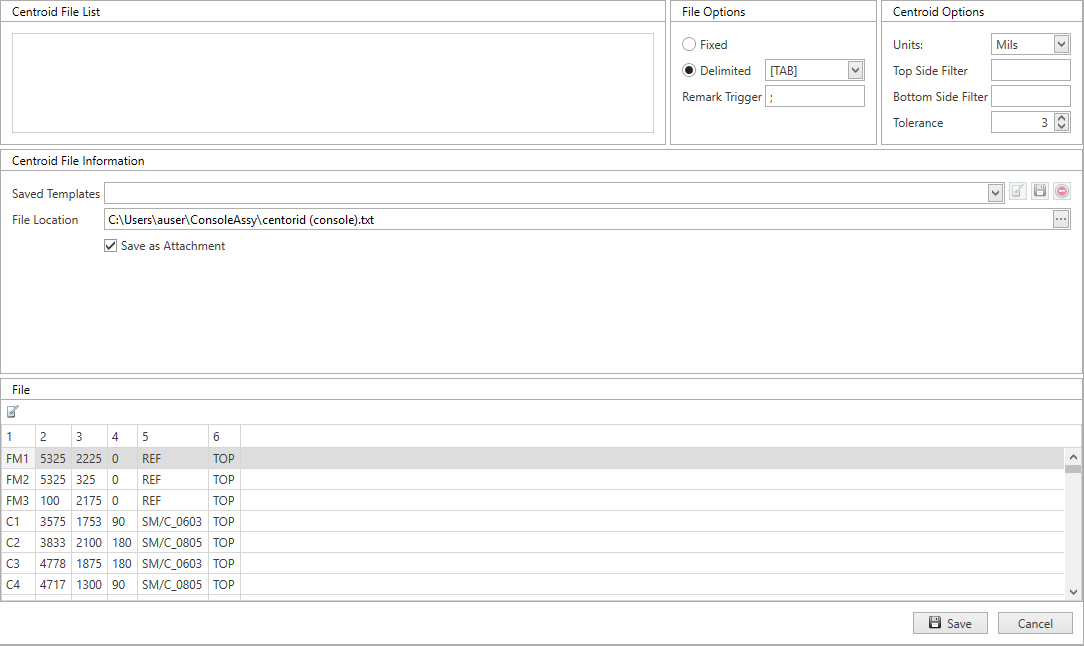 |

Use the Confirmations tools
Tool | Description |
|---|---|
Hide Digitized Features  | Hides all digitized components and features in the Gerber viewer. |
Accept All Components  | When selected, the system assigns all components in the buffer to their respective reference designators based on the loaded Centroid file. |
Accept Component  | When selected, the Commit Gerber Data dialog displays where you can assign reference designators to the all components in the buffer. |
Accept Board Frame  | Accepts the selected frame as the board frame. |
Digitize Gerber data
When you open a Gerber file for digitizing, FactoryLogix displays the top side Gerber layers by default.
Double-click ECAD in the Process tree to check out the Gerber file for digitizing.
Select the Digitize button on the Gerber toolbar.
Drag a rectangle around all of the features that make up a single component.
The selected component is highlighted along with any other component on the PCB that share the same footprint in a slightly darker color.Select the Accept Component button on the toolbar to open the Commit Gerber Data dialog. FactoryLogix will zoom in to the first part selected and prompt you to enter the reference designator for the highlighted part.
Enter the reference designator, then select the Accept button (check mark) to accept this component and advance to the next component in the Digitization Reference Queue. If an X/Y Centroid file was loaded earlier, FactoryLogix will automatically suggest the reference designator for the next component in the queue.
If the reference designator is correct, select the Accept Component button again to advance to the next part.
Continue accepting parts.
When you have accepted all parts in the digitization queue, FactoryLogix will return to the Gerber view and you can select a new component. Accepted components will change to a yellow highlight to indicate they are digitized.Repeat the steps to select and digitize components.
Since an X/Y Centroid file was loaded, you can speed up the digitization process by selecting a new footprint, then selecting the Select All Components button to accept all components in the digitization queue and assign reference designators from the X/Y Centroid File. As components are accepted, you can view the results on the PCB tab of the window.
To digitize the board frame for documentation purposes, select the Gerber tab, then select the Digitize Board Frame button. Hover over the Layers tab on the right side of the window to display the Gerber layers loaded in this assembly.
Set the Digitizable check box on the layer containing the board outline (usually an assembly drawing or silk screen layer). Select the board outline on the Gerber tab to highlight it.
To accept the selected outline as the board frame, select the Accept Board Frame button.
Select the padlock icon next to ECAD in the Process tree to save and check in your ECAD file changes.
When you are satisfied with the digitization, select the PCB tab to view the results.
Note
Use the zoom tools in the lower-right corner of the window to adjust the view of the PCB.

Gerber editing tools
The editing tools on the left side of the Gerber tab help you control the digitizing process, show and hide Gerber data, and make the digitizing process faster.
Icon | Tool | Description |
|---|---|---|
 | Single Select | Selects one or more parts. Ctrl+click to select multiple parts. |
 | Marquee Select | Selects one or more parts by dragging a rectangle around the desired parts. |
 | Lasso Select | Selects one or more parts by drawing an ellipse around several parts. |
 | Polygon Lasso Select | Allows for custom selection outlines. |
 | Hand Pan | Drag to move the ECAD. |
 | Selection Border | Specifies the line width of the border. 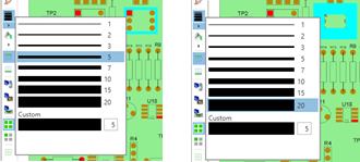 Select the Selection Border icon again after changing the border width when to show or hide the border around selected parts.  |
 | Selection Highlight | Specifies the highlight color for selected parts.  Select the Selection Border icon again after changing the border width to show or hide the border around selected parts.  |
 | View from Top | Sets the ECAD viewer to display the top-side parts. |
 | View from Bottom | Sets the ECAD viewer to display the bottom-side parts. |
 | Hide Gerber Inside a Rectangle | Hides all aperture data within a drawn rectangle. |
 | Hide Gerber Outside a Rectangle | Hides all aperture data from outside a drawn rectangle. |
 | Hide this Aperture | Hides the selected aperture. |
 | Align Layers | Aligns currently-selected layers. |
 | Reset Offset | Reverts offset Gerber layers back to their original loaded location. |
 | Selected Color | Indicates the currently-selected color. |
 | Select by Part | Selects all parts that have the same part number. |
 | Select by Footprint | Selects all parts that share the same Footprint. |
 | Select by Technology | Selects parts based on their installation method: SMT or through-hole. |
 | Show All Circuits | Sets the ECAD viewer to display all circuits of a panelized PCB. |
 | Show Root Circuit | Sets the ECAD viewer to display only the root circuit of a panelized PCB. |
 | Adjust Grid Spacing | Determines the spacing of the grid in the Gerber window. |
PCB tab editing tools
The PCB tab of the Process Definition window has powerful editing tools that allow you to edit PCB data. The tools are organized by type:
Search
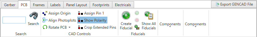
CAD Controls
Fiducials
Components (two sets of tools)
The following topics describe how to use the PCB tab's tools to modify PCB data.
Search for a reference designator
Use the Search tool to search for a specific reference designator on a PCB.
Tool | Description |
|---|---|
Search  | Searches the board for a specific reference designator.
|
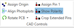
Use the CAD controls
Use the CAD Controls tools to assign the PCB datum (origin), align Gerber layers with the ECAD, rotate a board, and assign Pin 1.
Tool | Description |
|---|---|
Assign Origin | Defines the datum (0,0 point) of the board.
|
Align Photoplots | Lines up any associated Gerber layers with the ECAD. |
Rotate PCB | Adjusts the overall orientation of the board.
|
Assign Pin 1 | Defines which pin of a component is Pin 1. |
Show Polarity | Toggles the display of the red Pin 1 for each polarized component on/off. |
Crop Extended Pins | Crops all extended pins on the board. Warning |
Export GENCAD File 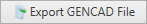 | Exports the selected data as a GENCAD file. |
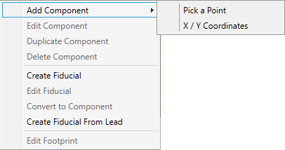
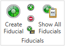
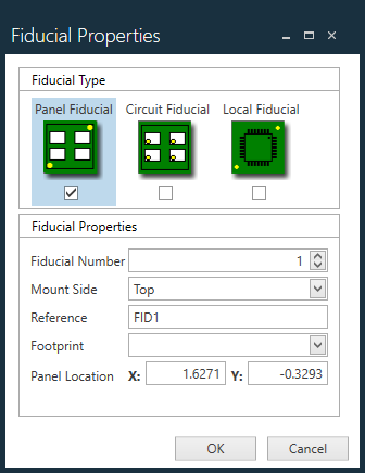
Modify fiducials
The Fiducials tools on the PCB tab of the NPI Process Definition window control every aspect of PCB fiducials. You can create and edit fiducials, hide or display, convert fiducials to components, and create fiducials from leads.
Tip
When creating or editing board components and fiducials, you can use the toolbar tools or right-click the board image in the window and use these menu commands:
Tool | Description |
|---|---|
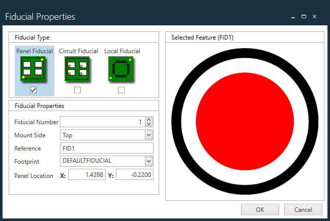
Create Fiducial | Adds fiducials to the board for machine programming purposes.
|
Edit Fiducial | Used to edit an existing fiducial.
|
Convert to Component | Converts a selected fiducial to a component. |
From Lead | Creates a fiducial from a selected existing component lead.
|
Show All Fiducials | Displays a table of all fiducials on the board. 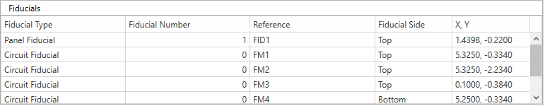 Select a fiducial from the table to see it in a zoomed-in view. |
Modify components
The two Components tool sets on the PCB tab of the NPI Process Definition window control every aspect of PCB components.
Tip
When creating or editing board components and fiducials, you can use the toolbar tools or right-click the board image in the window and use these menu commands:
Tool | Description |
|---|---|
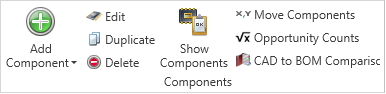
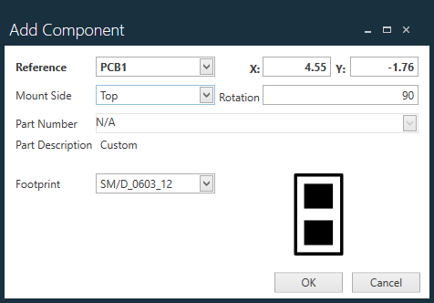
Add Component | Creates a new component location.
|
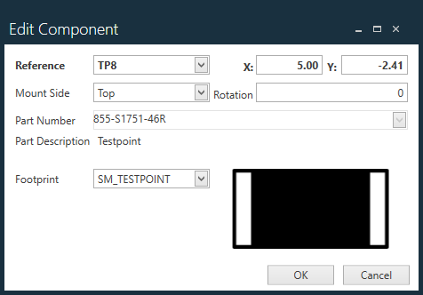
Edit | Modifies the basic properties of a selected component.
|
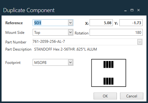
Duplicate | Creates a duplicate of the selected component.
|
Delete | Removes a selected component.
Warning Deleting a component cannot be undone! |
Show Components | Displays a table of all components on the board. Select Components, Show Components to display all of the board components. (Select Show Components again to hide the components.) 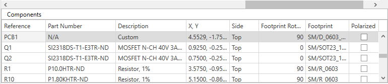
|
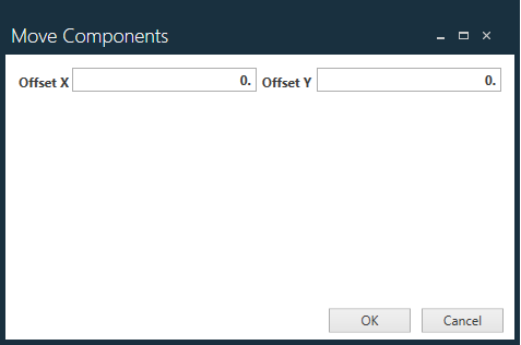
Move Components | Modifies a selected component to a new location on the board.
|
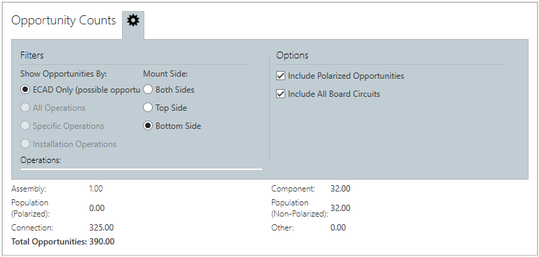
Opportunity Counts | Displays total opportunities for errors in the manufacturing process and options for reducing errors.
|
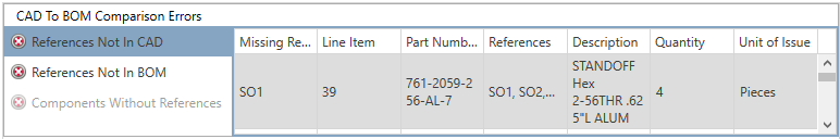
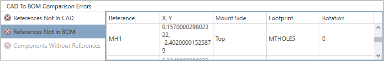
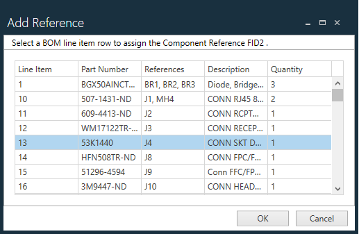
CAD to BOM Comparison | Displays discrepancies between the CAD and BOM so you can resolve errors before manufacturing the board. Resolve a CAD reference
Resolve a BOM reference
|
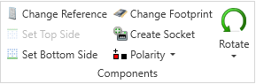
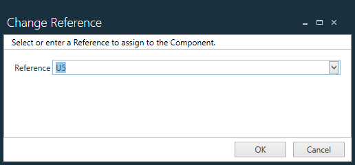
Change Reference | Modifies the reference for the selected component.
|
Set Top/Bottom Side | Modifies which side of the board the selected component is found (top or bottom)
|
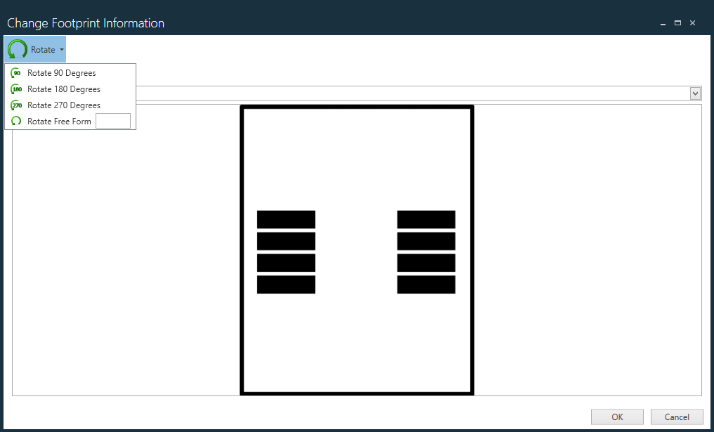
Change Footprint | Modifies the footprint shape used to represent a component.
|
Create Socket | Adds a new, slightly larger footprint around the selected part to represent a socket.
|
Polarity | Toggles the Polarized setting on/off.
|
Rotate | Changes the orientation of the selected component.
|

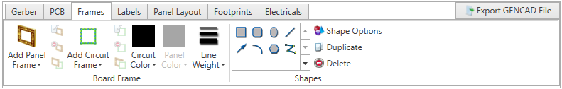
Create and edit PCB frames
Each PCB can have two frames or outlines: A panel frame and a circuit frame. On the Frames tab of the NPI Process Definition window, you can add panel and circuit frames to a PCB in case the ECAD data doesn't include frames. There are also tools to edit PCB frames including changing the frame or panel color and frame shape.
Frames tab editing tools
Tool | Description |
|---|---|
Add Panel Frame | Adds a panel frame to a PCB.
Note If you select a Rounded Rectangle frame shape, you are prompted to enter a corner radius value. 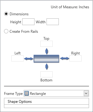
|
Edit Panel Frame | When selected, enables editing tools to modify frame properties such as shape, line weight, and color.
|
Delete Panel Frame | Deletes a selected panel frame from the board image. |
Copy Panel Frame to Circuit Frame | Copies a selected panel frame and its properties to a circuit frame. Note When you copy one frame type to another, the target frame is overwritten. |

Create and edit reference designator labels
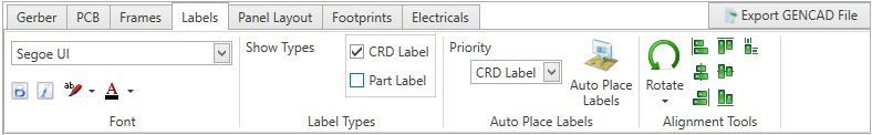
The Labels tab in the NPI Process Definition window allows you to change the appearance, size, and position of each reference designator on a PCB. The Auto Place Labels tool attempts to find the most suitable position and size. You can also enable Part Labels in addition to—or instead of—the CRD (Component Reference Designator) label with the Show Types options.
Labels tab editing tools
Tool | Description |
|---|---|
Font | Modifies the font, style, size, or color of selected reference designator labels. |
Label Types | Displays CRD labels, Part labels, or both. |
Auto Place Labels | Places labels on the board image automatically using optimal positioning. Before selecting Auto Place Labels, select a Priority from the drop-down to specify which label type should have priority over the other for label placement on the board image. |
Rotate | Rotates a label on the board image. Use Rotate Free Form to rotate selected labels using an angle you specify. |
Alignment Tools | Aligns selected labels on the board image. |
Edit the panel layout
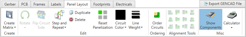
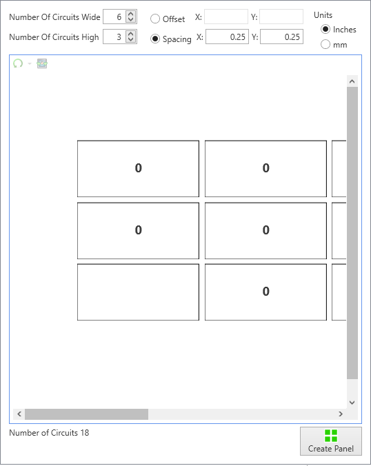
The Panel Layout tab in the NPI Process Definition window has tools to help you create a panelized assembly from a single-up (one-up) ECAD file. The Create Matrix tool defines the layout of the panel. It is also possible to create complex panel layouts with this tool such as panels with rotated or flipped circuits.
Panel layout tab editing tools
Tool | Description |
|---|---|
Create Matrix | Defines the layout of the panelized assembly you want to create from a single-up PCB ECAD file.
 |
Rotate | On a panelized layout, rotates selected board images a specified number of degrees. Use Rotate Free Form to rotate selected boards on the panelized layout using an angle you specify. |
Flip Circuit Side | Flips the circuit on selected board images. |
Step and Repeat | Creates a secondary matrix from one of the circuits already created with the Create Matrix option. For example, you would select this option if you needed to create a panel layout consisting of the original circuit, a circuit to the right in the X plane, and a circuit below on the Y plane (a 2x2 matrix without the diagonal circuit). In the dialog, you can set up the spacing and offset measurements. When you select the Create Panel button, the panelization is completed using the parameters you specify. 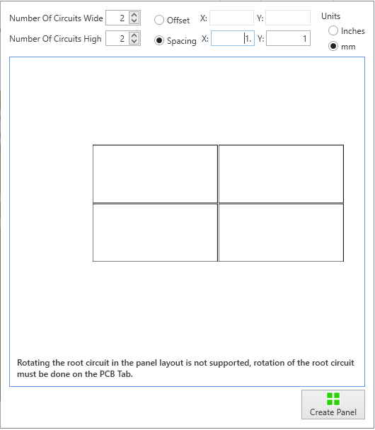 |
Duplicate | Duplicates selected circuits. |
Delete | Deletes one or more selected circuits on a panelized layout. (You cannot delete the root circuit.) |
Reset Panelization | Restores a panelized layout to a one-up board image. |
Circuit Color | Changes the color of the circuit. |
Line Weight | Modifies the line weight of the circuit. |
Order Circuits | Specifies the order of the circuits on a panelized assembly. Click a number to reset Circuit 1.  |
Alignment Tools | Aligns or distributes selected circuits on a panelized layout for optimal fit:
|
Show Components | Shows or hides all components on a panelized assembly. |
Calculator | Provides a calculator to use when working on panelized layouts.  |
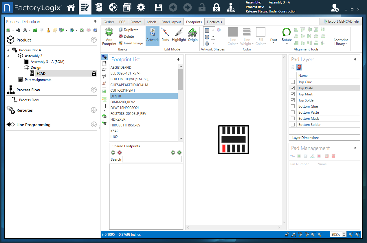
Modify footprints
The Footprints tab in the Process Definition window allows you to modify the graphical rendering of each component on the board. There are four aspects of each footprint that you can modify:
Artwork - Typically the overall outline or shape of the component footprint
Pads - Modifies the leads that make up the component, including reordering
Highlight - Modifies the area of the component used for color coding in Active Work Instructions
Origin - Changes the 0,0 (origin) point of a part

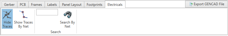
Modify electricals
There are currently three CAD file formats from which FactoryLogix can import Netlist and Trace information: GENCAD, PADS PowerPCB, and ODB++. You can use the Electricals tab in the Process Definition window to display these graphical traces.